It is the year of the microchip, and while the prevailing discussion revolves around shortages, advances in chipmaking techniques promise to revolutionise our gadgets.
The world’s largest chipmakers are promising significant performance and efficiency gains within the next decade, and they’re attributing them to the same method: transistor stacking.
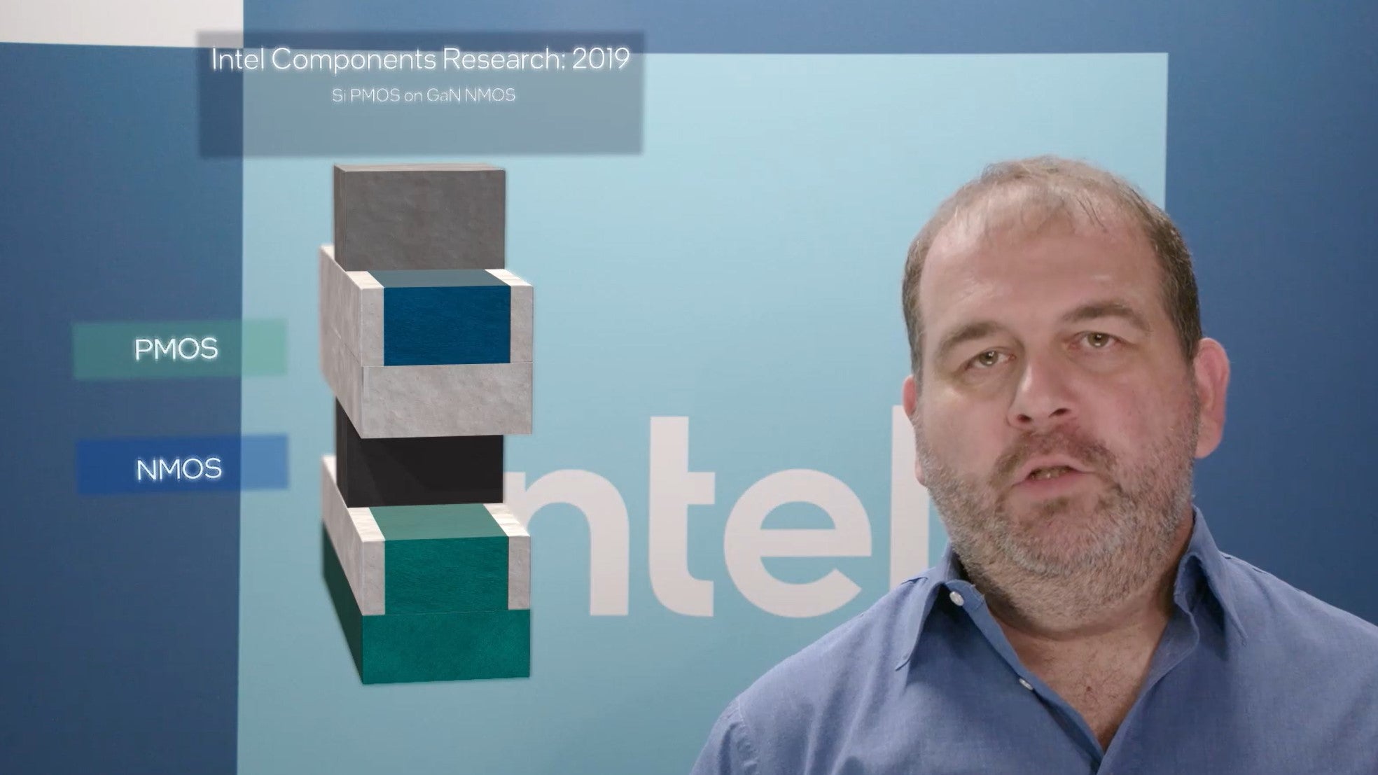
IBM and Samsung revealed during the IEDM conference in San Francisco a new technique for stacking transistors vertically, an approach the companies claim will either increase performance or boost efficiency. Separately, Intel described at the same conference a way of stacking transistors in a 3D orientation to fit more into a given space.
Intel frequently cites its desire to continue the trend established by Moore’s Law, a 1965 observation by Gordon Moore stating the number of transistors in an integrated circuit doubles about every two years. For decades, the semiconductor industry has operated on this premise, pushing to decrease die size every other year. However, the complexity of doing so has forced companies like Intel to delay moving to a more advanced microarchitecture. In Intel’s case, it meant falling behind the competition and losing high-profile customers, including Apple. With increasing difficulty to shrink dies, chipmakers are searching for new methods to upgrade the component at the heart of modern computing.
Today’s chips lie flat on the silicon surface, and current from metal layers flows horizontally to the source. Using the technique described by Samsung/IBM and Intel, the transistors would sit one above the other with current flowing vertically. Stacking NMOS and PMOS transistors on top of each other instead of placing them side by side could allow for a 30% to 50% increase in the number of transistors within a given area, according to Intel. More transistors means performing more complicated instructions.

“By stacking the devices directly on top of each other, we’re clearly saving area,” Paul Fischer, director and senior principal engineer of Intel’s Components Research Group, told Reuters in an interview. “We’re reducing interconnect lengths and really saving energy, making this not only more cost-efficient, but also better performing.”
Samsung and IBM, on the other hand, call their technology VTFET (Vertical Transport Field Effect Transistors) and claim it’ll be capable of offering 2x performance or 85% power efficiency improvements compared to FinFET designs. The companies say stacking allows them to overcome performance limitations or complete processes with less energy waste.
Here is the kicker: IBM and Samsung claim this could one day lead to smartphones that last a week on a charge, Engadget reports. And specific energy-sapping tasks like crypto-mining could see significant efficiency gains, an achievement that would reduce a massive carbon footprint.
We’re still in the early stages of this technology and several potential roadblocks will need to be addressed — thermal management being one of them — for this to be a viable solution. There is no timeline for when the first chips with vertically stacked transistors will arrive, but don’t expect it to be anytime soon. In 2011, Intel moved from flat MOSFET planar designs to FinFET, a 3D structure enabling better power efficiency.
Then earlier this year, Intel said it would move to a new transistor design called RibbonFET in 2024 with its Intel 20A chips. This upcoming structure uses ribbon-shaped channels surrounded by gates for faster performance in a smaller footprint. Vertical stacking would be a potential next step — one that could launch a new era of high-performance or low-energy computing.
