The elephant in the room has been, for a very long time, Moore’s Law, or really its eventual end game. Intel co-founder Gordon Moore predicted in a 1965 paper that the number of transistors on a chip would double each year. More transistors mean more speed, and that steady increase has fuelled decades of computer progress. It is the traditional way CPU makers make their CPUs faster. But those advances in transistors are showing signs of slowing down. “That’s running out of steam,” said Natalie Jerger, a professor of electrical and computer engineering at the University of Toronto.
Jerger’s not the only one saying it. In 2016, MIT’s Technology Review declared, “Moore’s Law is dead,” and in January of this year, the Register issued a “death notice” for Moore’s Law. And if you’ve purchased a laptop in the last couple of years, you’ve probably noticed it too. CPUs don’t seem to be getting that much faster year over year. Intel, which makes the CPUs found in the majority of our laptops, desktops, and servers, has rarely been able to boast more than a 15-per cent improvement in performance since 2014, and AMD, even with some rather radical new approaches to design, is typically only keeping pace with Intel in head-to-head battles.
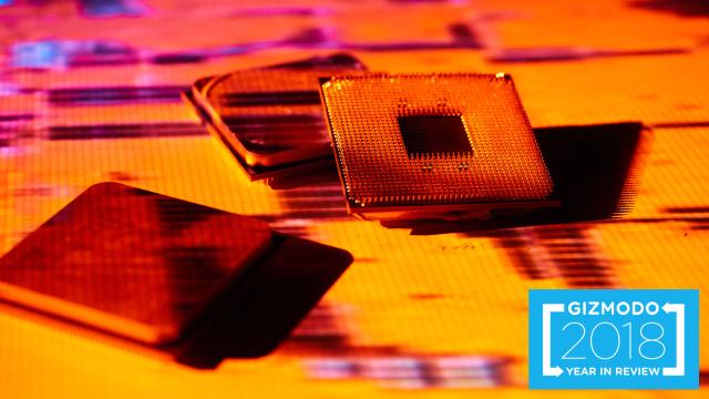
In the typical “monolithic” style of design incorporated by Intel and (until very recently) AMD, the CPU is composed of semiconductor material — almost always silicon. This is called the die. On top of the die are a series of transistors that communicate with each other quickly because they’re all on the same die. More transistors mean faster processing, and ideally, when you shrink the size of the die, the transistors are packed closer together and can communicate even more quickly with one another, leading to faster processes and better energy efficiency. In 1974, the very first microprocessor, Intel’s 8080, was built on a 6-micrometre die. Next year’s AMD processors are expected to be built on a 7-nanometre die. That’s close to 1,000 times smaller, and a whole lot faster.
But AMD achieved its biggest speed gains recently with its ridiculous-sounding Threadripper CPUs. These are CPUs with a core count that starts as low as 8 and goes all the way up to 32. A core is kind of like the engine of the CPU. In modern computing, multiple cores can function in parallel, allowing certain processes that take advantage of multiple cores to go even faster. Having 32 cores can take something like the rendering of a 3D file in Blender from 10 minutes down to only a minute and a half, as seen in this benchmark run by PCWorld.
Also, just saying you have a 32 core processor sounds cool! And AMD accomplished it by embracing chiplet design. All of its modern CPUs use something called Infinity Fabric. When speaking to Gizmodo earlier this year, this is what Jim Anderson, former general manager of AMD’s computing and graphics business group, called the “secret sauce” of AMD’s latest microarchitecture, Zen. CTO Mark Papermaster, meanwhile, dubbed it “a hidden gem.”
Infinity Fabric is a new system bus architecture based on the open source Hyper Transport. A system bus does what you think it would—bus data from one point to another. Infinity Fabric’s neat accomplishment is that it busses that data around really fast and allows processors built with it to overcome one of the primary hurdles of chiplet CPU design: latency.
Chiplet design isn’t new, but it’s often been difficult to accomplish because it’s hard to make a whole bunch of transistor on separate die talk to each other as quickly as they can on a single piece of silicon. But with AMD’s Threadrippers, you have a number of its typical Ryzen CPUs laid out on the Infinity Fabric and communicating nearly as quickly as if they were on a single die.
It works really well, and the results are a super-fast processor that is so cheap to make that AMD can sell it for a fraction of the price of something comparable from Intel—which continues to use monolithic design in its high-core-count CPUs. In a way, Infinity Fabric is a way to cheat Moore’s Law because it’s not a single fast CPU—it’s a whole bunch attached via the Infinity Fabric. So it’s not AMD overcoming the limitations of Moore’s Law, but circumventing it.
“If you step back in and say, ‘Well, Moore’s Law is really just about greater integration of functionality,’ I do think that the chiplets—it does not in any way help integrate more smaller transistors, but it does help us build systems that have greater functionality and greater capabilities than the generation before,” Jerger said.
She noted that in some cases, this conversation around chiplet design is a deflection from a company’s more notable failures. She’s referring to Intel, which has, for the last few years, notably struggled with the limitations of transistors that can’t shrink forever. It’s been stuck on a 14nm processor and promising, but failing to deliver, a 10nm processor for over a year. It’s been a terrible embarrassment for Intel that’s only been compounded as other chip makers have run laps around the incumbent chip giant. This year, Apple sold a few million phones and iPads with a 7nm processor inside, while AMD shipped 12nm processors and promised 7nm ones in 2019. AMD also publicly embarrassed Intel at Computex in Taipei this year: Intel promised a 28-core CPU by the end of the year (it still has not shipped), and days later AMD announced a 32-core CPU that has been shipping since August and costs half the Intel CPU’s forecasted price. Intel’s recent promise of a long-delayed shift to 10nm in 2019 looks kind of pathetic in comparison.
Which is why you shouldn’t view its embrace of chiplet CPU design as a coincidence. In part, this seems like Intel is talking up cool innovations to distract from a significant failure to innovate, or even keep up with the competition.
But as much as the chiplet stuff is about distracting from Intel’s 10nm problem, it’s also actually pretty damn cool. Intel’s first attempt at chiplet design was the relatively quiet launch of its G-Series CPU this past spring. That CPU was actually built in collaboration with AMD, which provided the GPU that Intel’s CPU would communicate with. Instead of relying on something like AMD’s Infinity Fabric, Intel developed something called the Embedded Multi-die Interconnect Bridge, or EMIB, that lets the CPU, GPU, and 4GB of High-Bandwidth Memory communicate at speeds approaching those of a series of components all on the same die. It’s fast for what it is, and we were suitably impressed when we tested it out back in March. It suggests a cool future where our integrated GPUs finally become as speedy as the discrete ones like Nvidia GTX and RTX series.
But EMIB was also like a testing of the waters for a product Intel announced earlier this month and expects to ship next year: a 10nm CPU with a chiplet design that incorporates 3D stacking. 3D stacking, like the EMIB, and like Infinity Fabric, is a tool of chiplet design. But where the Infinity Fabric and EMIB are just especially fast ways of making traditional CPU parts talk to each other more quickly, 3D stacking adds another dimension.
Typically chips are laid out on a horizontal plane so each part of the chip can make contact with the heatsink and keep nice and cool. 3D stacking, if the thermals can be handled correctly, allows you to build a CPU up instead of out. Sort of like a high rise versus a ranch-style home.
Intel’s really excited about 3D stacking—which it views as a more crucial circumvention of Moore’s Law than Infinity Fabric or EMIB. According to Intel’s Ramune Nagisetty, director of Process & Product Integration, it’s an “evolution” of Moore’s Law. Something she clarified in a conversation we had a few weeks ago:
“And you know if you take the time to dig up that original paper that Gordon Moore wrote. It’s really interesting because there is a paragraph in that paper where he actually foreshadowed this use of package integration. He didn’t use the same language that we use today, but he did say that it would prove to be more economical to build large systems of smaller functions which are separately packaged and interconnected.”
I’m not sure if I exactly agree with Nagisetty that it is an evolution, but she and Jerger both acknowledge that there is some flexibility in the language of that original paper by Moore, and that these package integrations (otherwise known as chiplet designs) do allow for new modes of CPU design beyond what Moore envisioned in 1965.
This year, we haven’t precisely seen the death Moore’s Law, but Intel and AMD know its fast approaching, and instead opted to think a little differently. Rather than make one single chip that will be incredibly fast and work for most people, these companies are now embracing a design that allows them to create a lot of smaller and more custom chips.
For Jerger, that flexibility is exciting. “Before it was all about kind of high volume—‘I have to build the thing that the most people want because that’s the only way I’m going to make any money.’ Now you can potentially be a lot more diverse, which I think allows academics and startups the opportunity to do some cool hardware design,” she said.
Imagine CPUs built specifically for your computer’s very exact needs. That’s the potential future we’re marching toward. And it all started with breaking the monolithic chip into chiplets.