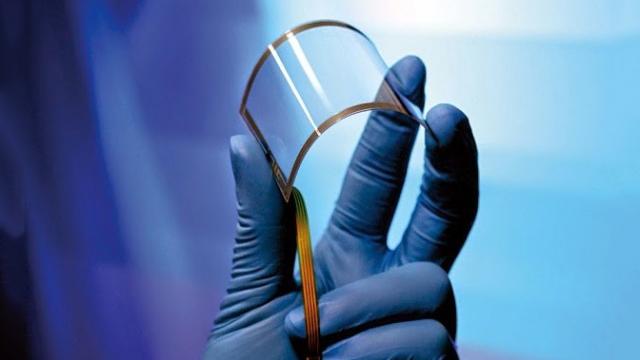
Graphene is regularly touted as a “super material” in electronics manufacturing — one able to do everything that silicon does, except better. But that isn’t good enough for one team at Berkeley Labs. They have combined graphene with two other cutting-edge materials to create the world’s first 2D field effects transistor. Your gadgets are about to get much, much faster.
A field effect transistor is a unipolar transistor and ubiquitous among modern personal electronic devices. It leverages an electrical field to control how charge carriers (electrons and holes) operate. This is opposed to conventional transistors that rely on tiny metal conduits laid down in the silicon wafer. An FET has three primary components: the source (where the electrons are coming from), a drain (where the electrons are going) and a gate (which acts like an on-off switch for the transistor, its position depending on the voltage applied). The problem with current generation of FETs is that flaws in the crystalline structures of these three components cause interference in the movement of electrons, which increases as voltages climb.
The Berkeley Lab’s new device is only six atomic layers thick — hence the 2D nomenclature — and leverages graphene as the gate, source, and drain; as well as hexagonal boron nitride (h-BN) as an insulator and molybdenite (molybdenum disulfide) as the channel. Each single-atom-thick layer was first mechanically exfoliated (shaved off a larger block of material) then laid carefully on a flexible silicon wafer. Van der Waal forces hold the six layers together rather than, say, chemical covalent bonds. Since each layer is individually generated and then placed on the substructure, researchers are able to minimize structural flaws at the molecular level.
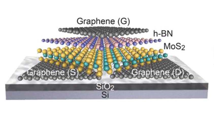
“In constructing our 2D FETs so that each component is made from layered materials with van der Waals interfaces, we provide a unique device structure in which the thickness of each component is well-defined without any surface roughness, not even at the atomic level,” Ali Javey, the project’s lead researcher said in a press statement. “The results demonstrate the promise of using an all-layered material system for future electronic applications.”
The 2D FET has already shown promise as a superfast transistor given it’s ability to rapidly cycle its gate (switch on and off) and unchanging electron mobility (how well electrons move from the source to the drain) at high voltages. This could lead to a new generation of ludicrously-fast CMOS chips that could boost the processing speed of mobile electronics by orders of magnitude. Of course, the technology will have to make the jump from lab to fab first. [Berkeley Lab via Extreme Tech – Wiki]